Capabilities & Technology
Pho-Tronics are experts at providing cost effective printed circuit board solutions since 1962.Pho-Tronics has been manufacturing rigid printed circuit boards since 1962; we are one of the oldest most experienced independent manufacturers of printed circuit boards in North America.
Pho-Tronics provides a wide range of manufacturing services from double sided to high layer count / high density multi- layer printed circuit boards. Pho-Tronics can seamlessly transition customers from quick–turn prototypes to cost effective volume production while mitigating risk and uncertainty.
Quality Certifications
ISO 9001-2015 Quality Management System
ITAR Approved
AS9100 Rev. D
IPC (Institute of Printed Circuits) Performance Standards:
IPC 1710 Company Profile
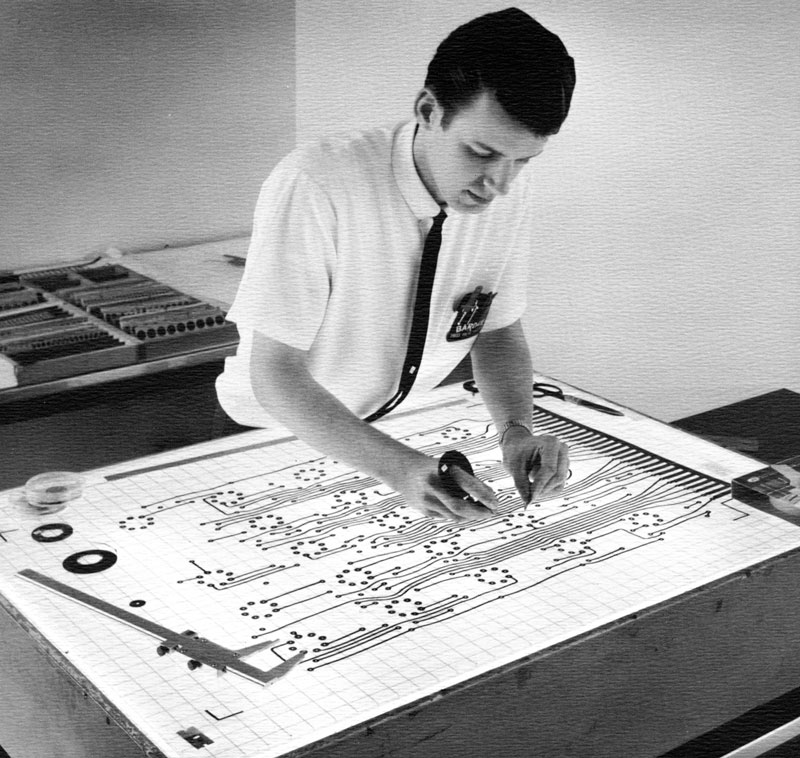
Bob Englehardt, Esq. – Circa 1966
Manufacturing Technologies
Multi-Layer Sequential Lamination
Hybrid Material Construction
Blind/Buried Vias
Edge Castellated Holes
Edge Plating
Heat Sink Bonding
Controlled Impedance
Metal Core Bonding
Precision Back Drilling
Edge Milling
Epoxy/Conductive Via hole fill
R/F Cavity Technology
Manufacturing Capabilities
| Manufacturing Features | Manufacturing Capabilities |
|---|---|
| I/L Trace and Space 0.5 oz. cu | .003/.003 |
| O/L Trace and Space 0.5 oz. cu | .003/.003 |
| I/L Etched Feature Tolerance {+/-} | .0005 |
| O/L Etched Feature Tolerance {+/-} | .001 |
| Smallest drilled via .062 thickness | .005 |
| Smallest drilled via .093 thickness | .008 |
| Smallest drilled via .130 thickness | .011 |
| IPC Class 2, {.001} Annular Ring O/L | .010 over finished hole size |
| IPC Class 3, {.002} Annular Ring O/L | .012 over finished hole size |
| IPC Class 2, {.001} Annular Ring I/L | .010 over drill diameter |
| IPC Class 3, {.002} Annular Ring I/L | .012 over drill diameter |
| Layer to Layer Registration {+/-} | .003 |
| Dimensional Feature to Feature {+/-} | .003 |
| Solder Mask Dam Width Min. | .003 |
| Solder Mask Clearance Tolerance {over pad} | .003 |
| Solder Mask Registration Tolerance | .002 |
| Plated Hole Tolerance {+/-} | .002 |
| Maximum Aspect Ratio | 12:1 |
| Maximum Board Thickness | .150 |
| Minimum Board Thickness | .016 |
| Minimum Dielectric Core Thickness | .002 |
| Maximum Layer Count | 24 |
| Maximum Panel Size | 21 x24 |
| Impedance Control Tolerance {+/-} Single Ended, Edge Coupled, Broad Sided Differential | +/- 7% |
| Maximum Bow and Twist | < 0.75% |
| Materials | |
| Polyimide | Yes |
| FR4, High TG | Yes |
| BT Epoxy | Yes |
| Low Loss | Yes |
| Halogen Fee | Yes |
| Surface Finishes | |
| HASL {Hot Air Solder Level} | Yes |
| Lead Free HASL | Yes |
| Immersion Silver | Yes |
| Immersion Tin | Yes |
| Immersion nickel gold {ENIG} | Yes |
| Electrolytic Plated Gold Tabs | Yes |
| Electrolytic Full Body Gold | Yes |
| Electrolytic Nickel | Yes |
| OSP {Organic Solderability Preservative} | Yes |
| Mixed Surface Finishes Example: Electrolytic Nickel And Enig | Yes |
| Special Processes | |
| Carbon Ink | Yes |
| Via Fill | Yes |
| Sequential Lamination | Yes |
Major Equipment
We are committed to providing defect-free products by adhering to the highest standards. To ensure our products satisfy our customers, our quality control systems focus on the most critical variables of each process.
All company personnel receive extensive training from basic techniques to advanced SPC techniques so that each operation is thoroughly examined. Each circuit board is studied from the inner layers to the surface, making sure each product is defect free before it leaves Pho-Tronics.
Drill / Routing Major Equipment
- Drill
- Posalux Ultra Speed 6000 – 6 station 220k RPM with control depth
- Posalux Ultra Speed 3600 – 2 station 160k RPM with control depth
- Excellon Mark VI – 4 station {2}
- Pluratec Inspectra D – 1 station X-Ray Drill with Diamond Vision
- Glenbook Real Time X-Ray
- Fabrication – Route
- AccuSystems AS-150 Max – V Jump Scoring System
- Micro – Vu Excel CMM 651 HC {Coordinate Measuring Machine}
- Excellon Mark VI – 4 station router
- Excellon Mark VI – 4 station router with control depth
- Excellon Mark V – 4 station router
- Excello XL 3 – 3 station Router {2}
Soldermask / Legend Print
- Soldermask
- Olec AccuTray AT 30 8 KW Auto Alignment Exposure System
- Olec AP 30 8 KW Exposure System
- Circuit Automation DP 1500 – 2x v 4.0 LPI {liquid photo imageable} Coating Machine
- Circuit Automation DP 10 Series 3 LPI {liquid photo imageable} Coating Machine
- Circuit Automation TC150 Tunnel Oven
- Circuit Chemistries VCM Vertical Soldermask Developer
- DynachemVacuum Lamination System
- Ceco Cyclops III Inspection System
- Dispatch Walk-In Convection Ovens {2}
- Sevecia Semi Automatic PC-B Screening Machine
- Colight UV 24 Soldermmask Cure Unit
- Schmid Combi Brush Jet Pumice Scrubber
- Legend Print / Screen
- Orbotech Sprint 100 Dual Head Ink Jet Legend Printer
Production Engineering – CAM
- Barco Ucamco Software
- Ucam: High performance CAM Station Printed Circuit Board {4}
- Ucam {X} Smart Test: Electrical Test – Net List Compare / Extraction Software
- Ucam SmartPlot: Plot queue Management Software for Photo-Plotter
- Ucam SmartAOI: Dedicated Secure Data Preparation Seat
- Prom’s ProCim Printed Circuit Board Manufacturing Solutions Software
Circuit Imaging
- Barco Silver Writer Laser High Resolution Photo Plotter
- Multi- Line 4 Slot Film Registration Artwork Punch
- Hakuto Cutsheet Film Resist Inner Layer Laminator with Wet Lam
- DuPont ASL Cursheet Film Resist Outer Layer Laminator
- DuPont “24” Hot Roll Film Laminator
- Chemcut 547 XL “30” Chemical Pre-Clean System
- Chemcut 547 Xli ’30’ Outer Layer Film Resist Developer
- ORC 5kw Double Drawer Exposure Unit
- Olec AP30 5KW Double drawer Exposure Unit
- Picard Glass Pin Registration Frames
- DuPont Silver Film Processor
Lamination
- Accudyne 150 Ton, 26 x 32, {6} Opening Vacumm Hydraulic Lamination Press
- Mac Dermid Conveyorized Multi-Bond Oxide Line
- PPSI 8 Camera Fixed Position Post Etch lamination Punch
- Multi-Line Post Etch Punch
- Despatch Walk-In Oven
- CECO Overhead Micrometer
- Multi-Line Lamination Plate Bridge Depinner
- Multi-Line Lamination Lay-up Station
- Somaca Lamination Plate Scrubber
- JJA Resin Spot Facer
- Excellon 4 Station Flash Router
- Ishi Hyoki Planerizer
Quality Control – Testing
- Inspection – Test
- Micro-Craft Flying Probe Electrical Tester EMMA – ELX6146
- Micro-Craft Flying Probe Electrical Tester EMMA – ELX6151
- Z-Metrix ST 600 Controlled Impediance Tester
- HY-POT Tester
- Camtek Orion PX AOI {Automatic Optical Inspection System}
- Fisher X-Ray Fluorescence Coating Thickness Measurement Instrument
- Micro-Section – Chemical Laboratory
- Nikon Epiphot Inverted Micro-Scope Scope with Dark Field and DIC {Differential Interference Contrast}
- Carl Zeisis Axio Vision Automatic Measurement Software for Printed Circuit Boards
- Unitron MEC 2 Inverted Microscope
- Buehler EcoMet IV Grinder-Polisher {3}
- Buck Instruments AA {Atomic Absorption Spectrometer}
- Chemical Anaylsis Software
Wet Process – Surface Finish
- Surface Finish
- Argus Vertical Hot Air Solder Leveler {HASL}
- ENIG Vertical Plating Line
- Immersion Silver Vertical Plating Line
- Baker Bros. MD 80 Gold Tab Plating System
- Wet Process
- Plasma Etch MK II 12 Slot Plasma Desmear System
- Hollmuller DES {Develop Etch Strip} Cupric Etcher
- Chemcut 547 XL DES {Develop Etch Strip} Cupric Etcher
- Chemcut 547 XL SES {Strip Etch Strip} Ammoniac Etch Line
- ASI 4 Brush De-Burr System with 1200 psi High Pressure Rinse
- Mac Dermid Conveyor zed Eclipse Direct Metallization Line
- ME Baker Automated Hoist PLC Controlled Desmear Electro-Less Plating line
- {1} 1200 gallon Dual Rectification electro-plate tin tank
- {2} 1200 gallon Single Rectification electro-plate copper tanks
- {1} 400 gallon Dual Rectification electro-plate tank
Here’s how we do it…
The process of checking for continuity and shorts on the boards by means applying a voltage between two points on the board. Depending upon the board complexity, this process may require a specially designed test fixture and test program for the electrical test system used by the board manufacturer.Process Flowchart
Download our process flowchart
“At Pho-Tronics it is not only what we do but how we do it that makes the difference”
In order to provide defect free product on time there has to be a laser focus on execution at every stage of the process. “Relentless Attention to Detail and Execution” is the foundation of the Pho-Tronics process and what differentiates us from the competition.
Pho-Tronics offers customers solutions that combine technological excellence with exemplarity customer service at an unparalleled competitive value. Our skilled engineering professionals are well qualified in assessing the feasibility of the design during the pre-production stage then determining the most cost effective manufacturing processes prior to production release.
The Pho-Tronics engineering service starts from the receipt of the electronic files and specifications. Engineering support services include impedance profiling, design for manufacturability, material selection and recommendation of alternative manufacturing solutions resulting in a robust printed circuit board.
1. Setup
The process of determining materials, processes, and requirements to meet the customer’s specifications for the board design based on the Gerber file information provided with the customer’s purchase order.
2. Imaging
This is the process of transferring the Gerber file data for a layer onto an etch resist film that is placed on the conductive copper layer.
3. Etching
The traditional process of exposing the copper and other areas unprotected by the etch resist film to a chemical that removes the unprotected copper, leaving the protected copper pads and traces in place; newer processes use plasma/laser etching instead of chemicals to remove the copper material, allowing finer line definitions.
4. Multilayer Pressing
The process of aligning the conductive copper and insulating dielectric layers and pressing them under heat to activate the adhesive in the dielectric layers, thus forming a solid board material.
5. Drilling
This is the process of drilling all of the various sized holes for plated through applications; a second drilling process is used for holes that are not to be plated through (see Step 7 below). Information on hole locations and sizes is contained in the drill drawing file.
6. Plating
The process of applying copper plating to the pads, traces, and drilled through holes that are to be plated through; boards are placed in an electrically charged bath of copper.
7. Second Drilling
This is required when holes are to be drilled through a copper area but the hole is not to be plated through (avoid this process if possible because it adds cost to the finished board through additional setup charges and labor).
8. Masking
This is the process of applying a protective masking material (solder mask) over the bare copper traces or over the copper that has had a thin layer of solder applied; the solder mask protects against environmental damage, provides insulation, protects against solder shorts, and protects traces that run between pads.
9. Surface Finish
The process of coating the pad areas with a very thin layer of solder to prepare the board for the eventual wave soldering or reflow soldering processes that will occur at a later date after the components have been placed.
10. Silk Screening
The process of applying the markings for component designations and component outlines to the board. May be applied to just the top side or to both sides if components are mounted on both top and bottom sides. Generally done in white non-conductive ink on the board surface.
11. Routing and Scoring
The process of separating multiple boards from a panel of identical boards; this process also allows cutting notches or slots into the board. Depending upon the size of the board, the entire panel of boards may be processed through the customer’s assembly, soldering, and testing processes and separated into individual boards at a later time.
12. Quality Control
A visual inspection of the boards; also can be the process of inspecting wall quality for plated through holes in multilayer boards by cross-sectioning or other methods.
13. Electrical Test
The process of checking for continuity and shorts on the boards by means applying a voltage between two points on the board. Depending upon the board complexity, this process may require a specially designed test fixture and test program for the electrical test system used by the board manufacturer.
Materials
Pho-Tronics Featured Performance Materials and Supplier Links
-
BT Resins
- Isola Group’s Bismaleimide/Triazine family G200 is a fully proven laminate and prepreg system designed to meet today’s high reliability printed circuit board requirements. Blending Bismaleimide/Triazine (BT) and epoxy resin provides G200 with enhanced thermal, mechanical and electrical performance over most epoxy materials. G200 possesses performance characteristics that make it an excellent selection for large panel size, high layer count Printed Wiring Boards (PWB) and HDI {High Density Interconnect} technologies. IPC-4101C /30. www.isola-group.com
- Nelco® N5000 BT epoxy laminate and prepreg system provides superior electrical properties. The N5000 resin system was originally developed for application specific use in high density military and commercial boards requiring not only close thickness tolerance, but also the ability to withstand the stress of multiple soldering excursions and repeated chemical exposure. www.parkelectro.com.
-
Epoxy Resins
- Isola 370HR is a high performance 180°C glass transition temperature (Tg) FR-4 system for multilayer Printed Wiring Board (PWB) applications where maximum thermal performance and reliability are required. 370HR provides improved thermal performance and low expansion rates in comparison to traditional FR-4 while retaining FR-4 process ability. In addition to this superior thermal performance, the mechanical, chemical and moisture resistance properties all equal or exceed the performance of traditional FR-4 materials. 370HR has proven to be best in class for sequential lamination designs.
- Nelco
N4000-29 is an advanced, lead-free, low-CTE, high Tg (185ºC by DSC) multifunctional epoxy dielectric substrate. This material has been designed for use not only in standard multilayer PWB designs, for today’s toughest, high-performance, lead-free applications.
- N4000-13 EP™ is an enhanced epoxy resin system engineered for today’s lead-free requirements where multiple solder reflow at temperatures approaching 260ºC are required. N4000-13 EP provides enhanced thermal reliability without compromising the electrical and signal loss properties that have made the Nelco® N4000-13 product family the industry standard for demanding high speed / low loss designs.
- The N4000-13 EP™ SI® is excellent for applications that require optimum signal integrity and precise impedance control, while maintaining high CAF resistance and thermal reliability.
- Iteq IT-180ABS/IT-180ATC
IT-180A is an advanced high TG {175 C by DSC}, multifunctional epoxy with low CTE, high thermal reliability and CAF resistance. It is designed for high layer count printed circuit boards and can pass 260 C Lead free assembly and sequential lamination process. www.iteq.com
-
Polyimide Resins
- Isola P96/P26 product line of polyimide-based prepreg and copper-clad laminates for high-temperature printed circuit applications. These products consist of a polyimide resin system suitable for applications requiring superior performance and the utmost in thermal properties. These products utilize a polyimide and thermoplastic blend resin, fully cured without the use of Methylenedianiline (MDA). This results in a polymer with a high Tg without the characteristic difficulties of brittleness and low initial bond strength associated with traditional thermoset polyimides. www.isola-group.com
- The Nelco N7000-1 series of polyimide laminate and prepreg has a low Z-axis expansion and high-Tg offering consistent board performance and reliability. N7000-1 is a good choice for applications requiring the superior thermal stability and chemical resistance provided by a polyimide. www.parkelectro.com.
-
RF Materials
- Rogers Corporation | www.rogerscorp.com
RO3000® high frequency circuit materials are ceramic-filled PTFE composites intended for use in commercial microwave and RF applications. This family of products was designed to offer exceptional electrical and mechanical stability. RO3000 series laminates are circuit materials with mechanical properties that are consistent regardless of the dielectric constant selected. This allows the designer to develop multi-layer board designs that use different dielectric constant materials for individual layers, without encountering warpage or reliability problems. The dielectric constant versus temperature of RO3000 series materials is very stable.
- RO4000® hydrocarbon ceramic laminates and pre-pregs offer superior high frequency performance and low cost circuit fabrication resulting in a low loss material which can be fabricated using standard epoxy/glass (FR-4) processes. RO4000 material possesses the properties needed by designers of RF microwave circuits and matching networks and controlled impedance transmission lines. RO4000 series laminates offer a range of dielectric constants (2.55 – 6.15), are available with UL 94 V-0 flame retardant versions
- RO4350B™ materials are proprietary woven glass reinforced hydrocarbon/ceramics with electrical performance close to PTFE/woven glass and the manufacturability of epoxy/ glass. Providing tight control on dielectric constant and low loss while utilizing the same processing method as standard epoxy/glass, RO4350B is available at a fraction of the cost of conventional microwave laminates. No special through-hole treatments or handling procedures are required as with PTFE based microwave materials. RO4350B materials are UL 94V-0 rated for active devices and high power RF designs.
- Nelco
The Nelco® N4350-13 RF and N4380-13 RF series are enhanced epoxy resin systems specifically engineered to provide a unique solution for design applications that demand outstanding thermal properties, tight dielectric constant tolerances and low signal loss properties. These next generation modified epoxies combine tightly controlled RF electrical properties with the mechanical reliability and competitive advantages of FR-4. www.parkelectro.com